(Singapore)

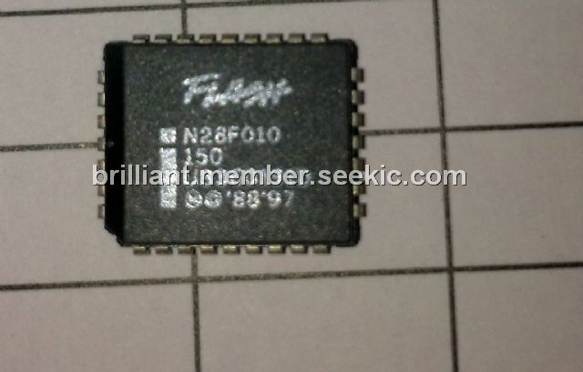
Product Summary
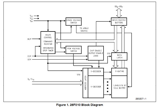
The N28F010-150 is a flash memory. The device offers the most cost-effective and reliable alternative for read/write random access nonvolatile memory. The N28F010-150 adds electrical chip-erasure and reprogramming to familiar EPROM technology. Memory contents can be rewritten: in a test socket; in a PROM-programmer socket; on-board during subassembly test; in-system during final test; and in-system after-sale. The N28F010-150 increases memory flexibility, while contributing to time and cost savings.
Parametrics
N28F010-150 absolute maximum ratings: (1)Operating Temperature, During Read: 0 to 70℃; During Erase/Program: 0 to 70℃; (2)Operating Temperature, During Read: 0 to 85℃; During Erase/Program: -40 to 85℃; (3)Temperature Under Bias: -10 to 80℃; (4)Temperature Under Bias: -50 to 95℃; (5)Storage Temperature: -65 to 125℃; (6)Voltage on Any Pin with Respect to Ground: -2.0V to 7.0V; (7)Voltage on Pin A9 with Respect to Ground: -2.0V to 13.5V; (8)VPP Supply Voltage with Respect to Ground During Erase/Program: 2.0V to 14.0V; (9)VCC Supply Voltage with Respect to Ground: -2.0V to 7.0V; (10)Output Short Circuit Current: 100 mA.
Features
N28F010-150 features: (1)Flash Electrical Chip-Erase: 1 Second Typical Chip-Erase; (2)Quick Pulse Programming Algorithm: 10 μs Typical Byte-Program; 2 Second Chip-Program; (3)100,000 Erase/Program Cycles; (4)12.0V ±5% VPP; (5)High-Performance Read: 65 ns Maximum Access Time; (6)CMOS Low Power Consumption: 10 mA Typical Active Current; 50 mA Typical Standby Current; 0 Watts Data Retention Power; (7)Integrated Program/Erase Stop Timer; (8)Command Register Architecture for Microprocessor/ Microcontroller Compatible Write Interface; (9)Noise Immunity Features: ±10% VCC Tolerance; Maximum Latch-Up Immunity through EPI Processing; (10)ETOXTM Nonvolatile Flash Technology: EPROM-Compatible Process Base; High-Volume Manufacturing Experience; (11)YEDEC-Standard Pinouts.
Diagrams